![]() Introduction to Photolithography
Introduction to Photolithography
Slideshow
Edit
1. Introduction to Photolithography
2. The Photolithography Process
3. Types of Light in Photolithography
4. Wavelength and Feature Size Relationship
5. Photolithography: Cleaning and Preparation
6. Application of Photoresist
7. Exposure and Developing
8. Etching in Photolithography
9. Photolithography Exposure Systems
10. Resolution in Projection Systems
11. Light Sources and Innovations
Overview of Photolithography
1. Introduction to Photolithography
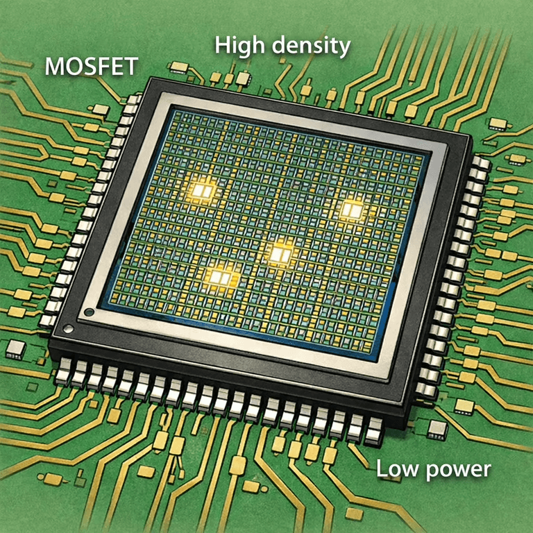
Photolithography transfers patterns onto silicon wafers using light, crucial for integrated circuits in microfabrication.
2. The Photolithography Process
Involves cleaning wafers, applying photoresist, exposure to light, and developing to transfer patterns onto wafers.
3. Types of Light in Photolithography
Ultraviolet, deep UV, EUV, and X-ray lithography are used, with the wavelength impacting feature size.
4. Wavelength and Feature Size Relationship
Loading equations
Photolithography Steps
5. Photolithography: Cleaning and Preparation
Silicon wafers are cleaned and prepared with an adhesion promoter for photoresist application.
6. Application of Photoresist
Photoresist is applied onto wafers via spin coating, creating a uniform layer for pattern exposure.
7. Exposure and Developing
Light exposure changes photoresist properties, allowing development to reveal the pattern.
Pattern Transfer Techniques
8. Etching in Photolithography
Etching removes material from unprotected areas, crucial for pattern transfer in microfabrication.
Advanced Concepts in Photolithography
9. Photolithography Exposure Systems
Use of photomasks in projection systems to pattern wafers efficiently in semiconductor fabrication.
10. Resolution in Projection Systems
Loading equations
11. Light Sources and Innovations
EUV and laser technologies improve resolution for smaller feature sizes in integrated circuits.


 Introduction to Photolithography